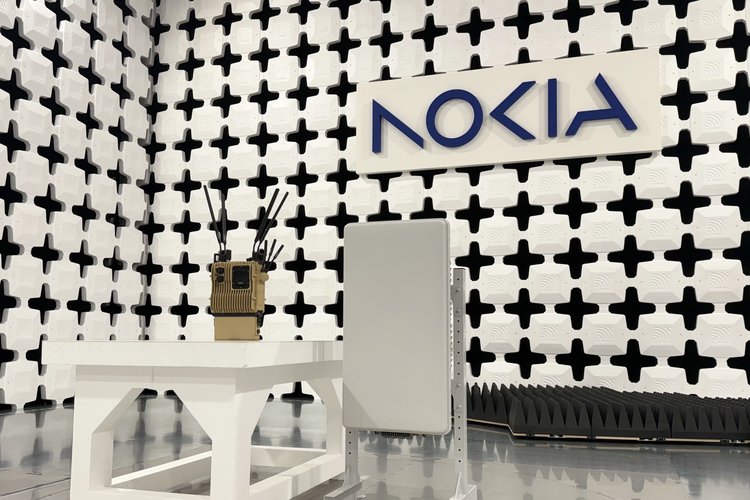
Nokia is set to ramp up operations at its advanced test and packaging (ATP) facility in Allentown, Pennsylvania, with a major expansion set to bolster its optical networking production capacity.
The expansion will see the Finnish firm invest $30 million, which includes around $4 million in assistance from the state of Pennsylvania and $10 million in federal investment tax credit via the CHIPS Act.

Nokia said the effort will almost double its Pennsylvania workforce to more than 500 jobs spanning engineering, manufacturing, and R&D, with a projected economic impact of more than $500 million over the next five years.
Currently, less than two percent of global semiconductor ATP takes place in the US at Nokia’s Allentown facility. But the vendor claimed its expansion will increase the site’s production capacity by up to 10 times its current level, with new capacity expected to be commercially available by the end of the third quarter.
“The AI supercycle is fundamentally reshaping network and infrastructure requirements in the US and globally,” said Nokia president and CEO Justin Hotard. “Our expansion in Allentown is a direct investment in that future – scaling domestic manufacturing of the optical networking technologies that power AI infrastructure.”
The expansion comes as part of Nokia’s pledge to invest $4 billion in R&D and manufacturing in the US. Among its ongoing efforts are building a new home for its Bell Labs arm, moving it from its iconic Murray Hill home to a more modern facility in New Brunswick, and the creation of a fab in San Jose, California, to bolster its Infinera efforts.
Bolstering manufacturing capacity for its optical technologies is key for Nokia, given the growing importance of advanced connectivity solutions for both its telecom and data center-focused offerings.
Its optics lines have quickly become a key growth driver, with its recent earnings revealing the segment alone providing a revenue bump of 20 percent.
But the move also comes as a growing number of silicon-related players are shifting manufacturing capacity to the US in the wake of tariff threats from the Trump administration, with Nokia joining Apple, Taiwan Semiconductor Manufacturing Co. (TSMC), and Nvidia in pledging to manufacture stateside.
“Nokia’s investment in Pennsylvania is directly advancing America’s AI leadership,” said Bill Frauenhofer, executive director of semiconductor investment and innovation at the Department of Commerce.
“Supported by CHIPS and Science Act funding, Nokia is deepening its commitment to innovation and the production of photonic chips in the United States. This project enables critical optical technology and strengthens America’s semiconductor supply chain.”


More in The Compute, Storage & Networking Channel


Read the orginal article: https://www.datacenterdynamics.com/en/news/nokia-to-scale-optics-manufacturing-in-with-30m-expansion-in-pennsylvania/


