It may prove to be more economical to build large systems out of smaller functions, which are separately packaged and interconnected,” Gordon Moore wrote in his famous article, Cramming more components onto integrated circuits, describing the concept that would come to be known as chiplets.
Moore’s article was published in 1965. The concept of chiplets is not a new one, even if the term used to describe the technology is a more recent adoption.

Issue 57 – A French Revolution
The fight to become Europe’s AI infrastructure capital
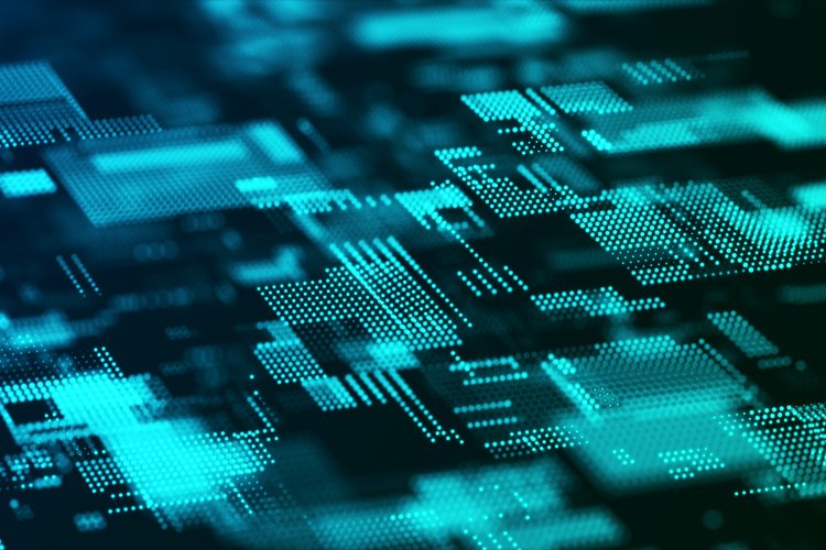
On a basic level, chiplets are tiny integrated circuits with specialized functions, which can be combined to make larger integrated circuits that are then packaged and sold as a single component.
Unlike a system-on-a-chip (SoC), which is monolithic and integrates all its system components onto a single silicon die, chiplets are modular, comprising smaller interconnected dies that can be easily scaled through the addition or removal of chiplets. As a result, they provide a number of benefits over monolithic dies, including greater flexibility, faster time to market, lower costs, and improved yields, and have enjoyed a resurgence in popularity in recent years.
However, while chiplets might allow for a more efficient use of resources and improved performance, there is still one major disadvantage: their complex interconnect design. While companies had previously tried to overcome this challenge, true interoperability had been largely lacking.
Enter Universal Chiplet Interconnect Express (UCIe), set up by a consortium of chip industry giants in March 2022 to establish a standardized open specification for interconnects between chiplets.
The primary drivers for the standardization were the need for performance, power efficiency, and the ability to handle different process nodes, says Debendra Das Sharma, Intel senior fellow and chairman of the UCIe consortium since its inception.
Initially founded by 10 members, including AMD, Arm, Microsoft, Qualcomm, and TSMC, the consortium now has 12 promoter companies and lists more than 84 contributor members on its website.
“If you look into the industry landscape, everyone is doing chiplets,” Das Sharma says. “If you look into server offerings, GPU offerings, CPU offerings, you name it, everyone is doing chiplets and putting together multiple chiplets and packaging them and interconnecting them in some way.”
Das Sharma notes that there are a number of key drivers of this trend, the primary one being that chip manufacturers are starting to hit the limit of how much they can grow one die. There’s also the ever-increasing need for performance and power efficiency.”
“The need is such that you need the bigger dies, you need more functionality coming out into the packet,” Das Sharma explains. “And the way to do that is by getting multiple chiplets and connecting them in some way to make it look like one big chip.”
Another reason chiplets have grown in popularity is that they provide companies with the ability to create bespoke solutions.
“You can do mix and match,” Das Sharma says. “For example, I can have an accelerator of a given cloud service provider in my offering, but someone else might want a different type of accelerator and still want it to look like it’s a heterogeneous computing package.
“You can have different types of accelerators, you can have a different number of cores, different amounts of memory, all serving different people for different usages. And chiplets allow you to do that. You can put two of these, three of the other type, five of something else, you can do the mix and match and get your own solution.”
Das Sharma also explains that different process nodes, used in the production of chips, are better at different things. Memory, for example, is best produced on its own process node, separate from compute, while IO can be produced more effectively on less advanced nodes.
“There are different flavors of process technology for different types of usages,” he says. “There’s no reason you can’t put everything on one die, but it’s not going to do very well. So, that’s the other reason people do chiplets.”
The UCIe 1.0 specification was released in March 2022 and defined the physical layer, protocol stack, software model, and compliance test procedures. The UCIe 1.1 specification followed in August 2023 and included architectural specification enhancements, simultaneous multiprotocol support, and new bump maps in an effort to lower packaging costs.
A year later, in August 2024, the UCIe 2.0 specification was released, bringing with it support for 3D packaging, improved system-level solutions, optimized package designs, and full backward compatibility with UCIe 1.0.
Dr. Ian Cutress, chief analyst at More Than Moore, says that, at present, there’s a lot of money going into chiplet-related technologies, especially through startups. However, he cautions that while they can provide great advantages, chiplets aren’t perhaps quite the silver bullet the industry is searching for, and UCIe is actually only one part of a much larger puzzle.
“What we are talking about is incredibly complex and more expensive than older technologies that may already exist but may not be universal standards,” Cutress says.
“Advanced packaging is expensive, leading-edge chips are expensive, putting them together is expensive, validating the whole set is expensive. The whole concept of chiplets, in and of itself, is difficult, because if you’ve got a design made up of chiplets, which one is the control? Which one’s managing the power? How do you cool it? What’s the right thermal environment? Where are the hot spots? What’s the validation? These are all important questions, but UCIe only attacks the one thing, and that’s how the chips communicate with each other? All the rest of it still needs to be solved by whoever’s building the chip.“
Optical illusion
While UCIe was established in 2022, it’s only in more recent years that hardware vendors have started to release technology based on the specifications, largely because vendors such as Synopsys or Cadence have started to provide IP offerings.
The Synopsys product, announced in September 2024, consists of a complete UCIe IP solution, operating at up to 40Gbps, faster than the industry standard.
“Our active contribution to the UCIe consortium has enabled us to deliver a robust UCIe solution that helps our customers successfully develop and optimize their multi-die designs for high-performance AI computing systems,” Michael Posner, VP of IP product management at Synopsys, said at the time.
Das Sharma says that one of the tenets of the UCIe standard is that it should leverage existing packaging technologies. Because different companies have their own bump technologies, the UCIe standard accommodates these variations, with the focus being on defining the interconnect and ensuring compatibility with existing manufacturing processes.
He also described the consortium as being “forward-looking” when it introduced the specification in 2022, with a statement proclaiming that optical and co-packaged optics would be the means by which people will communicate, because it offers a lot of bandwidth within a very tight form factor.
“If you look at the amount of bandwidth we offer as UCIe, it’s a lot,” Das Sharma says. “Our power numbers on UCIe are fairly low, so it’s a fairly good match in the sense that we are going to define things on the UCIe interface that means you can bring in your optical technology, and we are not going to constrain you about what kind of optical technology… we just want to define a common interface on UCIe that will work with any optical technology.”
Ayar Labs is one such company that has already developed optical UCIe interconnect technology.
Unveiled at 2025’s Optical Fiber Communication Conference (OFC) in San Francisco, the company describes its offering as the world’s first UCIe optical interconnect chiplet.
Combining silicon photonics with CMOS manufacturing processes to support the use of optical interconnects in a chiplet form factor within multi-chip packages, the chiplet is powered by Ayar Labs’ 16-wavelength SuperNova light source and is capable of achieving 8Tbps bandwidth.
The company says its compatibility with the UCIe standard helps to create a more accessible, cost-effective ecosystem, streamlining the adoption of advanced optical technologies necessary to scale AI workloads while overcoming the limitations of traditional copper interconnects.
Aside from the excitement of getting to work alongside the members of the consortium, Terry Thorn, vice president of commercial operations at Ayar Labs, says that the company wanted to develop UCIe-based technology because it was a “very natural growth path for us.”
“The fact that a lot of companies were endorsing and adopting UCIe… it just made a lot of sense for us to go that direction. So that’s what we did.”

Ayar Labs taped out its UCIe optical interconnect chiplet in 2024, with Thorn saying that, as a result of being part of the consortium, the company has been able to work with a number of firms that have also adopted the technology in both the pre and post-silicon phases of its chip development.
In the pre-silicon phase, he said Ayar Labs was able to line up test bench structures based on UCIe specifications to see that its chips would work together when they came back from the fabs, while post-silicon – the phase the company is in now – it has paired the chips up and see that they are connecting how they’re supposed to.
“That’s actually not simple to do if you’re not working from a standard,” he says.
“On the electric interface side, if you’re going to build a co-packaged optics or you’re going to build a fully optical system, there are a lot of things that have to be considered in order to do that, things like package and test.
“How do you architect and design the light source into the system? We use an external light source, which allows us to do things on a separate part of the rack, but all of that has to be considered as you start to build out fully optically enabled AI systems.”
Thorn says that, as a standards-based approach, UCIe brings great benefits.
He continues: “When you look at the adoption of UCIe across the companies that have joined the consortium and are endorsing it, it really just eases the adoption from a chiplet standpoint, in a really significant way, because each customer may have some level of chiplet performance or chiplet customization they want, but you’re still going back to that standard interface on the electrical side, so that that certainly helps you in addressing their needs.”
Despite a number of UCIe-focused announcements made in the wake of OFC – Lightmatter also launched photonic interconnects at OCP that “use a standard interoperable UCIe die-to-die interface to facilitate scalable chiplet-based architectures” – Cutress says that the move towards optical interconnects isn’t necessarily going to be a big driver of UCIe technology in the immediate future.
“Optics on its own doesn’t amplify UCIe in any way; however, UCIe can amplify optics medium to long term,” he says.
“The reason is that the optics industry, especially co-packaged optics, is still fairly nascent. I have a few clients in this space, and you know they’re all saying 2027-2029 is more the time frame they’re targeting, but for non-UCIe optics.
“What UCIe brings to the table is that with most optics solutions, whether you’re going chip to chip or chip to memory, you have to connect the ASIC, your AI chip, to an optics engine, and one of the ways to connect to that optics engine is through UCIe.”
Cutress says that most optics deployments that have been unveiled already, such as Nvidia’s switches or Marvell’s data center interconnect modules, are not using UCIe, but are instead relying on proprietary protocols.
“UCIe does help standardize that interface as we start to have more players in the optic space,” he adds. “There are companies designing the optics connections and other companies designing the AI ASIC, and at some point, they have to decide what connections they’re going to use if they plan to work together.
“If they both support UCIe, then it’s a plus. But optics is still a bit far out, and it’s not necessarily a driver of UCIe, although UCIe could help the medium to long-term adoption of optics in the industry.”
The next spec
Looking to the future, Thorn says that Ayar Labs’ first effort with UCIe, what is referred to as the standard package, will be its immediate focus, with an advanced package offering targeted for the following years.
“I would say in 2025 and going into 2026 we’re really focused on the standard package approach and what we can do with it, and what our partners can get done with it, both pre-silicon and post-silicon,” he says. “I would say the coming year, year plus, our roadmap starts to look at ‘how would you implement and how do you position the value add of advanced package UCIe?’”
Meanwhile, Das Sharma, who teases that fresh UCIe news might be on the horizon – “the journey continues and we will have something exciting to be talking about pretty soon” – says the regular cadence of releases for new UCIe specifications has been in response to demand.
Meanwhile, Das Sharma, who teases that fresh UCIe news might be on the horizon – “the journey continues and we will have something exciting to be talking about pretty soon” – says the regular cadence of releases for new UCIe specifications has been in response to demand.
“There is so much pent-up demand, but in general, we always try to do a spec release based on real demand,” he explains. “And invariably, what happens is we have more requests than we can handle. So, it’s always a matter of prioritizing things. Something goes out now, something else will go out a little later, and so that’s what drives the cadence. Right now, we have no shortage of ideas about what to do and what to pursue, and we all know, in this business, there is no dull moment.”
However, Cutress says that while he expects to see a lot more demos regarding the technology’s interoperability in the coming year, especially from startups and small to mid-sized companies, he’s unsure when companies will begin to announce UCIe has been built into chips being used in actual products.
While companies like Nvidia, AMD, and Intel have all shown chiplets and prototypes that demonstrated the practical application of UCIe, Cutress says the likes of Broadcom or Marvell, which have ASIC design teams building chips for hyperscalers, never comment on their customers or talk about what technologies are used inside those chips.
“UCIe, in itself, isn’t designed to be a marketing body,” he says. “Would the consortium like to talk about partners who have delivered UCIe solutions? Yes. Will those partners want to tell their competitors they’ve enabled this, that, or the other? No.
“It’s quite possible there are actually UCIe technologies, maybe in some embedded use case, or some networking appliance that’s actually in a data center somewhere in the Middle East, but we don’t know.”
Without wanting to speculate on why companies do certain things, Thorn says the lack of transparency around the deployment of this technology likely relates to the fact that it’s still relatively early days for UCIe.
“They want to make sure their designs are performant to the degree that they want them to be, and that they can do it in volume before they tend to say anything public about it. That’s my suspicion,” he says.
“I don’t know, it’s up to them, but [Ayar Labs] takes comfort in the fact that the majority of the conversations we have are rallying around the UCIe interface and what’s happening in that space.”


Read the orginal article: https://www.datacenterdynamics.com/en/analysis/making-connections-the-pursuit-of-chiplet-interconnect-standardization/


