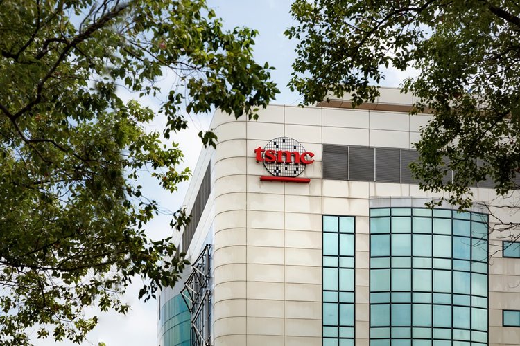
TSMC is planning to open a chip design center in Munich, Germany.
The company announced the facility during its European Technology Symposium in Amsterdam, the Netherlands, this week.
The center will support European customers in designing high-density, high-performance, and energy-efficient chips, with a focus on automotive, industrial, AI, and IoT applications, president of TSMC Europe, Paul de Bot, told attendees, in comments reported by Reuters.
TSMC currently has nine other chip design centers across the world, located in Canada, China, Japan, Taiwan, and the US, but the Munich facility will be the company’s first in Europe.
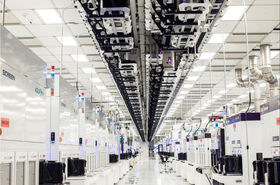
Germany is also home to TSMC’s first European chip fab, currently under construction in Dresden. Dubbed ESMC (European Semiconductor Manufacturing Company), the facility is a collaborative effort between TSMC and NXP, Infineon, and Bosch, with the European trio each owning a 10 percent stake in the plant.
The total cost of the project is expected to be more than $10bn, with the plant due to be operational by 2027. When complete, the site will produce 40,000 wafers a month. However, TSMC has previously said the fab will not be used to manufacture the company’s most cutting-edge chips, instead focusing on 28nm, 22nm, and 16/12nm nodes.


Read the orginal article: https://www.datacenterdynamics.com/en/news/tsmc-to-open-chip-design-center-in-munich-germany/


